Remarks as a Guide to Digital Clock #001 Assembly
The page is prepared for the readers who consider making a set of the present digital clock.
The author will give in this page many remarks including commonsense matters, which may be
helpful for beginners. However, the design is somewhat complicated and this clock seems not
so suited for beginner's subject.
Remarks related to the style of schematic drawings.
- ICs.
The IC package option is assumed to be DIP for most devices, TO-92 for LM285-2.5/LM385-2.5
shunt reference, or TO-220 for 78M05/7805 3-terminal regulator in drawing schematics.
The ICs are depicted from top view or from front view, and the pin #1 is marked with
a circle in the scematics.
- 7-segment LED display units.
In terms of pin assignment, the 7-segment LED disply units are drawn consistently with
the front view of standard single-digit 7-segment LED units of 14.2mm (0.56 inch)
character height. However, it is advised in any case to refer to the datasheet of the
devices you will use.
- Resistors.
The nominal resistance value of the resistors are designated in ohms. For example,
2.2 stands for 2.2 ohm, 10k stands for 10 kiro-ohm, and 10M stands for 10 meg-ohm.
- Capacitors.
The nominal capacitance value of the capacitors are designated in farads, and the character u
denotes micro (i.e., the greek letter mu). For example, 1000p stands for 1000 pico-farad,
and 0.1u stands for 0.1 micro-farad.
- Decoupling capacitors (bypass capacitors).
Although they are often not drawn in the schematics, a decoupling capacitor of
0.01uF to 0.1uF should be placed across the supply pins of each logic IC. In the present
design, all the ICs depicted with 14 or 16 pin outline are all of the logic ICs used.
For these 14 pin ICs (namely, 74HC20 (U2) and 74HC132 (U3,U4,U5)),
supply pins are assigned to the pins #7 and #14.
For these 16 pin ICs (namely, 4521B (U1), 74HC390 (U6,U7) and 4511B (U8,U9,U10)),
supply pins are assigned to the pins #8 and #16.
- Decimal points in the schematics.
Sorry, the decimal points appearing in the present schematics (files sd030**.gif) are
very small (it seems a dot of single pixel). Please read schematics carefully with
sufficient magnification of viewer.
Component choice.
- LEDs.
Choose LEDs by which adequate brightness is obtained at the forward current
of (static) 5mA or less for each LED segment.
The restriction to 5mA/segment is related to the capacity of power supply section.
It is also recommended to choose LEDs showing forward voltage drop of less than about 3V.
- 7-segment LED display units.
The 7-segment LED units must be of common-cathode type.
Be sure to choose simple common-cathode units (multiplex or dynamic-drive display units,
which are often found among 4-digit LED display units designed for digital clocks,
cannot be used in the present clock).
See also the above-described remarks for LEDs, which applies to 7-segment LED units too.
- Resistors.
Low-cost 5% tolerance, 1/4 watt carbon film resistors can be used unless otherwise noted.
- The LED current limitting resistors.
In the schematic SD03020 of display section, resistance value of the LED current
limitting resistors is not designated. To determine the resistance value RLIM,
use the equation
RLIM = (4.3V - VF)/IF
where IF is the required LED current par segment and VF the forward
voltage drop of the LED.
For example, if an LED segment requires IF = 4.5mA and the voltage drop
of VF = 2V develops at the LED, then use of RLIM = 510 ohm resistor
is in order.
- Capacitors.
- capacitors for which polarity (+/-) is specified in the schematic.
Use of aluminum electrolytic capacitors of standard class is in order. The voltage value
designated in the schematic is minimum requirement of rated voltage.
- capacitors of 100pF or less capacitances.
Use of C0G (or NP0 in other words) characteristic, 5% tolerance 50V ceramic capacitors
is in order.
- decoupling capacitors (capacitors not explicitly drawn in the schematics).
It is enough to use low-cost Y5V characteristic, 25V to 50V rated voltage,
+80%/-20% tolerance ceramic capacitors (slightly expensive X5R or X7R characteristic
units can also be used).
- other capacitors.
Use of 25V to 50V rated voltage, 5% to 20% tolerance
ceramic capacitors of X5R, X7R or C0G (NP0) characteristic is recommended
(polyester film capacitors can also be used instead) unless otherwise noted.
- Transistors (this remark is written especially for the readers in Japan).
Toshiba 2SC1815-Y or 2SC1815-GR can be used in place of the 2N3904 transistor
in the present design.
Toshiba 2SA1015-Y or 2SA1015-GR can be used in place of the 2N3906 transistor
in the present design.
It should be mentioned that these transistors are all molded in the same outline
(TO-92 package), but the pin assignment differs between 2N3904/2N3906 and 2SC1815/2SA1015.
- Pushbutton switches.
Choose pushbutton switches or tact switches of normally-open
momentary types (those turn on during and only during they are pushed).
- Power transformer and fuse holder.
Choose chasis mount style units rather than PCB mount
ones as far as possible (see the following remark for reason).
Remarks for safety and reliablity.
- Particular attention should be paid for insulation at the AC power line or primary side
of the power transformer for safety. Insulation between pads/traces/wires on prototype-style
circuit board to which high voltage applies cannot easily be kept good and reliable for long time.
Therefore, wiring from the AC power input to the primary winding of power transformer is
recommended to be made entirely outside the circuit board, as a simple but relatively safe method.
- Wiring of the power lines Vcc and GND among the ICs is preferably done with multiple paths
forming many loops. Further, avoid use of unnecessarily long interconnect wire for signal lines.
These apply also to the
interconnects between separated schematics (e.g., wires connecting the circuit of
schematics SD03010 and the circuit of schematics SD03020 should not also be unnecessarily long).
However, wires around the power transformer, wires connected to the pushbutton switches
and wires connected to the LEDs can be somewhat long without problem.
- In assembly of the circuit, the aluminum electrolytic capacitors are recommended to be
discharged before they are settled into the circuit.
- Fast lowering (at the rate in excess of 5V par 1ms) of supply voltage (voltage between
Vcc and GND lines) may damage some ICs, through which some capacitor's discharge current flows.
Such a condition does not arise in normal use of the clock, but may occur if connection of
some component (in particular a capacitor) to the circuit is established while power is
supplied to the circuit, or if Vcc and GND lines are shorted together accidentally or
intentionally, probably in debugging an assembled set.
Attention should be paid to avoid realizing such a condition in particular in debugging
the circuit.
Circuit board assembly example photoes.
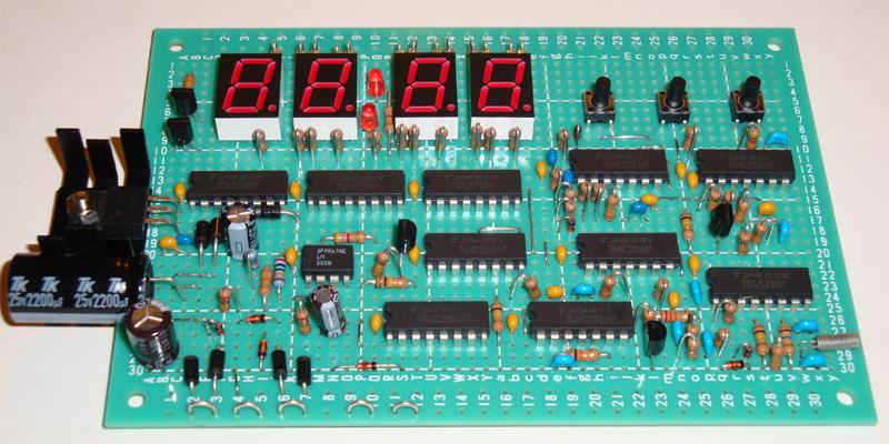
All components except for power transformer, fuse, fuse holder, 9V battery and battery snap
are mounted on a single prototyping board.
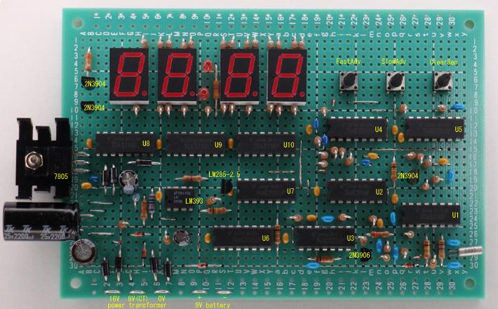
Component side photo.
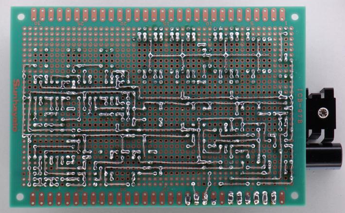
Solder side photo before wiring by wire-wrap wires is made.
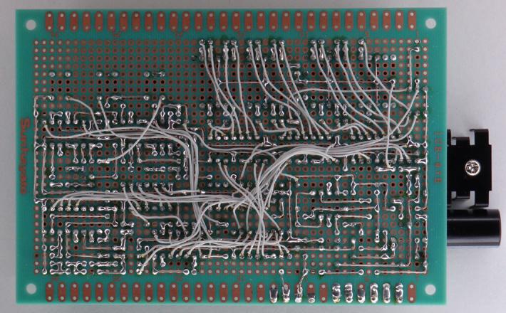
Solder side photo when wiring completes (wire-wrap wires are also soldered).
Homepage URL: http://www.uranus.dti.ne.jp/~n-sasaki/